CH-RTF/反转铜箔
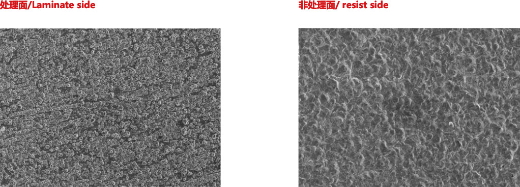
通过特殊的表面处理工艺,将电解铜箔S面进行精细瘤化处理,有效降低铜箔与基材接触面 的轮廓,降低PCB端产品应用中的电信号损失,可应用5G高频高速领域。/Through the special
post-treatment process, the electrolytic copper foil S surface is coarsened and solidified to reduce the profile of the contact surface between the copper foil and the substrate, to
reduce the letter loss in the application of the PCB end product, and to expand the application field of the PCB end product.
• 铜箔与基材结合面轮廓度低,PCB端蚀刻出现残铜导致短路状况改善明显,并且微蚀速度提 升。/Copper foil and substrate surface profile is low, PCB end etching residual copper
leads to obvious improvement of short circuit, and micro corrosion speed.
• PCB端铜箔M面可直接贴附干膜,不需要太多处理即可有良好的结合力,降低PCB端断路风 险。/The M surface of PCB copper foil can be directly attached to the dry film, without too
much treatment, it can have good adhesion and reduce the risk of open circuit of PCB .
产品/技术优势/Advantages of Product/ Technology
良好的高温延伸率/Good high temperature elongation
• 改善PCB端断路、短路异常/Improvement of open & short problems in PCB .
• 微蚀速度提升,具有良好的蚀刻因子/The micro etching speed is increased and the etching factor is effective.
• 信损低/Low signal loss
• 多种规格型号供客户选择/Various specifications and models for customer selection
产品/技术应用范围Application Area(s) of Product/ Technology
5G通讯等电子信息产业发展高速印制电路板/5G Communications and Electroni9c Information Industry Development of High Speed Printed Circuit Boards
代表特性数据/Representive date


总部地址:广东省梅州市梅县区宪梓南路19号超华科技大厦
电话 Tel :86-753-8586699 传真 Fax :86-753-8592000

扫描关注
超华官方公众号

扫描关注
超华投资者关系公众号
总部地址:广东省梅州市梅县区宪梓南路19号超华科技大厦
电话 Tel :86-753-8586699
传真 Fax :86-753-8592000
版权所有 © 广东超华科技股份有限公司 1996-2019 保留一切权利

